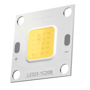
High-performance custom indicators, light-emitting modules, and specialty sensor devices engineered for industrial efficiency.
Bridging the gap between raw silicon processing and next-generation optical intelligence across global industries.
Autonomous mobility demands high-speed, high-density sensor feedback. Our custom SMT photodiode arrays act as core receivers in LiDAR flight-time calculations, enabling precise 3D environmental mapping under high ambient light conditions.
From pulse oximeters to clinical lab analyzers, our surface mount photodiodes are customized for exact quantum efficiency peaks at specific biological absorption wavelengths, ensuring high signal-to-noise ratios (SNR).
Integrating high-speed PIN photodiodes into smart factories allows for real-time laser alignment, high-frequency optical switching, and precise positioning in high-speed pick-and-place lines.
An analytical breakdown of current market trends, supply chain positioning, and materials engineering shift.
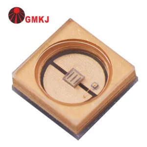
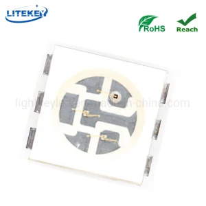
The optoelectronics market is experiencing a profound architectural pivot. Traditional leaded (through-hole) photodiodes are rapidly being phased out due to physical space constraints and the requirements of automated high-speed surface-mount technology (SMT) reflow assembly. Industrial buyers and engineering firms are actively seeking highly customizable OEM/ODM suppliers capable of producing miniature photodetectors that do not compromise on sensitivity or thermal robustness.
Currently, the market demands silicon-based photodiodes for visible to near-infrared spectrum ranges (400nm - 1100nm), and InGaAs (Indium Gallium Arsenide) for short-wavelength infrared (SWIR) detection. The challenges in sourcing premium wafers, coupled with strict packaging tolerances, require a vertically integrated manufacturing process. Manufacturers must maintain cleanroom environments class 10,000 or better to prevent microscopic dust contamination, which can directly cause elevated dark current levels and component failures in field operations.
Precision optical tailoring designed to meet exact customer specifications.
We match target wavelengths by modifying silicon doping depths and utilizing integrated optical bandpass coatings. Our capabilities range from deep UV monitoring to near-infrared ambient light rejection.
Balancing dark current, junction capacitance, and response speed. Our engineers tailor active area footprints (from 0.1 mm² to over 15 mm²) to fit perfectly within compact SMT system footprints.
Supporting high-temp ceramic packages, standard FR4 substrates, or transparent epoxy molds. We build custom-shaped sub-assemblies to handle critical board layout designs.
Zhongshan Zever Light Co., Ltd.
Zhongshan Zever Light Co., Ltd. was established in 2005 and is a professional LED manufacturer located in Zhongshan, China—one of the country’s key lighting industry hubs.
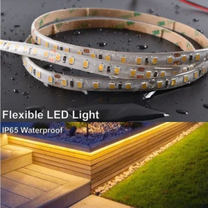
We specialize in the research, development, production, and sales of a wide range of LED products. Our main product lines include THT LEDs, SMD/Chip LEDs, LED displays, infrared LEDs, dot matrix modules, LCD backlights, and various LED lighting fixtures for commercial and residential applications.
With advanced automatic production equipment and modern manufacturing technology, we ensure high efficiency and consistent product quality. Our factory operates under strict quality management systems and has been certified with ISO9001 and ISO14001 standards.
Our facility covers approximately 6,000 square meters and is equipped with 8 production lines, supported by a skilled workforce of over 800 employees. All raw materials we use comply with RoHS directives and are sourced from reliable suppliers in Taiwan, the United States, Japan, and South Korea to guarantee superior performance and environmental safety.


At Zever Light, we place strong emphasis on innovation and customization. Our dedicated R&D team, consisting of 16 experienced engineers with an average of more than 5 years in the LED industry, is capable of meeting both standard and highly customized requirements. We welcome customers’ ideas and designs and are committed to turning them into high-quality, market-ready products.
Our management system is supported by an advanced ERP platform, ensuring efficient operations and on-time delivery. Our quality control team conducts strict inspections at every stage—from incoming materials to production and final shipment—to ensure that every product meets international standards.
We pride ourselves on fast delivery times, with urgent orders fulfilled in as little as 1–2 weeks. Our commitment to reliability, quality, and customer satisfaction has earned us the trust of clients worldwide.
Quality is our culture.
Working with us means your investment is secure and your business is supported by a dependable partner.
Zhongshan Zever Light Co., Ltd. looks forward to building long-term partnerships and creating a brighter future together. For inquiries about our LED and Photodiode custom products, please contact us today.
Aligning manufacturing capabilities with local market regulations, physical delivery workflows, and environmental certifications.
Our strict adherence to international environmental directives ensures smooth imports. We certify that all surface mount photodiodes are Lead-Free, RoHS, and REACH compliant. We implement rigorous component screening to support halogen-free manufacturing goals.
Sourcing raw wafers and chip components from trusted wafer foundries in Japan, South Korea, Taiwan, and the US enables us to manage supply chain risks. Through our ERP platform, we maintain buffered inventory stocks for repeat OEM accounts.
Innovating today to prepare for the integrated electro-optical architectures of tomorrow.
As micro-assembly limits scale downward, Zever Light's R&D roadmap focuses on two core fields: Silicon Photonics integration and Multispectral Filter arrays. Integrated packaging techniques allow photodiodes to be assembled side-by-side with laser emitter diodes or within miniature system-in-package (SiP) environments. This proximity reduces stray signal capacitance, pushing operational frequency limits past several gigahertz.
Additionally, we are expanding our cleanroom capacities to integrate direct-on-chip optical filtering processes. By sputtering thin-film interference filters directly onto the surface mount photodiode wafers, we eliminate the need for secondary optical glass covers. This significantly lowers overall profile dimensions, resulting in high optical clarity and excellent durability in tough industrial environments.
Resolving common layout, material properties, and operational parameters queries.
Q1: How do surface mount photodiodes compare with traditional through-hole configurations in terms of performance?
A1: Surface mount (SMT) photodiodes dramatically lower parasitic inductance and capacitance due to shorter signal routing paths. This reduction translates directly to faster rise times (often < 5ns) and higher operating bandwidths, which are essential for optical communication links and high-speed laser scanners.
Q2: How does Zever Light control Dark Current in customized OEM photodiode arrays?
A2: Dark current is minimized by using high-purity silicon wafers and implementing strict guard-ring structures within our silicon fabrication steps. Additionally, our automated die attachment and strict ISO-certified cleanroom packaging prevent surface contaminants that could otherwise cause leakage currents.
Q3: What thermal parameters must be considered during the SMT reflow soldering process?
A3: Our surface-mount photodiode packaging is built to survive peak lead-free reflow temperatures of up to 260°C for a duration of 10 to 20 seconds. We suggest following standard IPC/JEDEC J-STD-020 profiles to maintain package integrity and prevent thermal stresses.
Q4: Can Zever Light provide custom optical filters directly integrated into the photodiode encapsulation?
A4: Yes. Through our advanced ODM services, we offer daylight blocking filters that filter out visible light while letting near-infrared light (850nm - 940nm) pass through. Alternatively, we can apply custom bandpass coatings for specific measurement wavelengths.
Q5: What is the typical lead time for custom OEM prototypes compared to bulk production runs?
A5: Custom layout prototyping and wafer engineering iterations typically take between 4 to 6 weeks, which includes tool creation and custom test setup. Once designs are approved, our 8 automated production lines can ship production orders within 2 to 3 weeks.
High-quality components for medical equipment, solid-state curing, and custom opto-electronic setups.